Skip to content
Meiwafosis Co., Ltd.
- Company Name:
- Meiwafosis Co., Ltd.
- Representative's name:
- Location:
- 1-14-2, Shinjuku Shinjuku-ku Tokyo 160-0022 Japan
- Tel:
- +81 3 5379 0051
- Fax:
- +81 3 5379 0811
- E-mail:
- infot@meiwanet.co.jp
- URL:
- http://www.meiwafosis.com/
- Products:
- Osmium Coater, Carbon Coater, Soft Plasma Etching Device
- Sales Points:
- Overseas Distribution Partners Wanted/OEM Options Available
Meiwafosis Co., Ltd. has been developing, manufacturing, exporting, importing and selling research instruments, analyzers, optical instruments and electronic equipment in Japan since the foundation of the company in 1968.
We are currently looking for overseas distribution partners for our own instruments: “Osmium Coater”, “Carbon Coater”, and “Soft Plasma Etching Device”. OEM options are also available. If you are interested, please feel free to contact us.
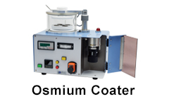
- Osmium Coater
Its ultra-thin film deposition (1nm-) enables you to observe the original structure of a sample. It prevents electron beam damage without inducing charge-up even on complicated surface structures, and it does not cause damage to samples even if they are weak to heat. No graininess is seen even in high-magnification images. Our Osmium Coater provides better-quality deposition than sputter coaters. Ideal for SEM observation and pretreatment for various element analyses (EDS, AES, XPS, EBSD, etc.). More than 300 units have been sold both within and outside Japan so far.
- Carbon Coater
It has a plasma treatment function. Since plasma treatment and carbon deposition can be conducted under the same vacuum environment, it allows hydrophilic treatment to be done right after coating in a continuous process. It only takes about 5 minutes to finish the whole process (from setting to coating). As ultrapure carbon fiber (99.995%) is singly used for each deposition, there is no risk of residue of impurities. Ideal for SEM observation, EDS analysis, FIB protective films and various analyses. More than 280 units have been sold both within and outside Japan so far.
- Soft Plasma Etching Device
Its low voltage plasma treatment makes it suitable for sensitive samples that would be easily damaged by high-power. Impurities can be removed (cleaned) without using heat treatment or organic solvents. Since our specially-designed electrodes equally cover 80% of the sample stage, large samples can be thoroughly processed as well. Ideal for hydrophilic treatment, surface modification, contamination removal for SEM samples, and PDMS bonding. More than 150 units have been sold both within and outside Japan so far.
Dry etching has typically been done on large high frequency equipment. However, dry etching can be done by our new bench-top type high output model with CF4 gas. It irradiates a stable 1000V of plasma and can handle difficult samples such as TiO2 in a short processing time.
- Images:
-